Boise State’s second annual Research Month is April 2018. Research Month celebrates the diverse and fascinating array of research happening each day on campus.
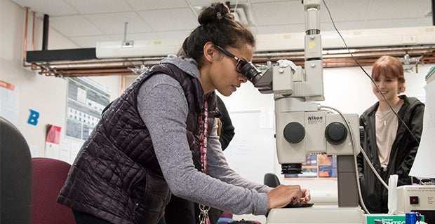
In Boise State University’s Surface Science Lab, managed by lab engineer Paul Davis, clinical assistant professor Harold Ackler’s students take turns examining and creating maps of surfaces with a resolution approximately 100,000 times smaller than the width of a human hair.
The process is called atomic force microscopy (AFM), a form of scanning probe microscopy (SPM) that works by scanning a very sharp needle (the “probe”) over the surface of a sample, mapping out its hills and valleys to create a 3D topographical map of the surface. As Davis and Ackler explain, the AFM process differs from a standard light microscope in that instead of shining light on a sample and focusing a magnified image of it onto a viewer’s eyes, like in a regular optical microscope such as one might use in biology class, an AFM “sees” the surface by “feeling” it – similar to a person reading Braille – and generates a magnified image on a computer screen.
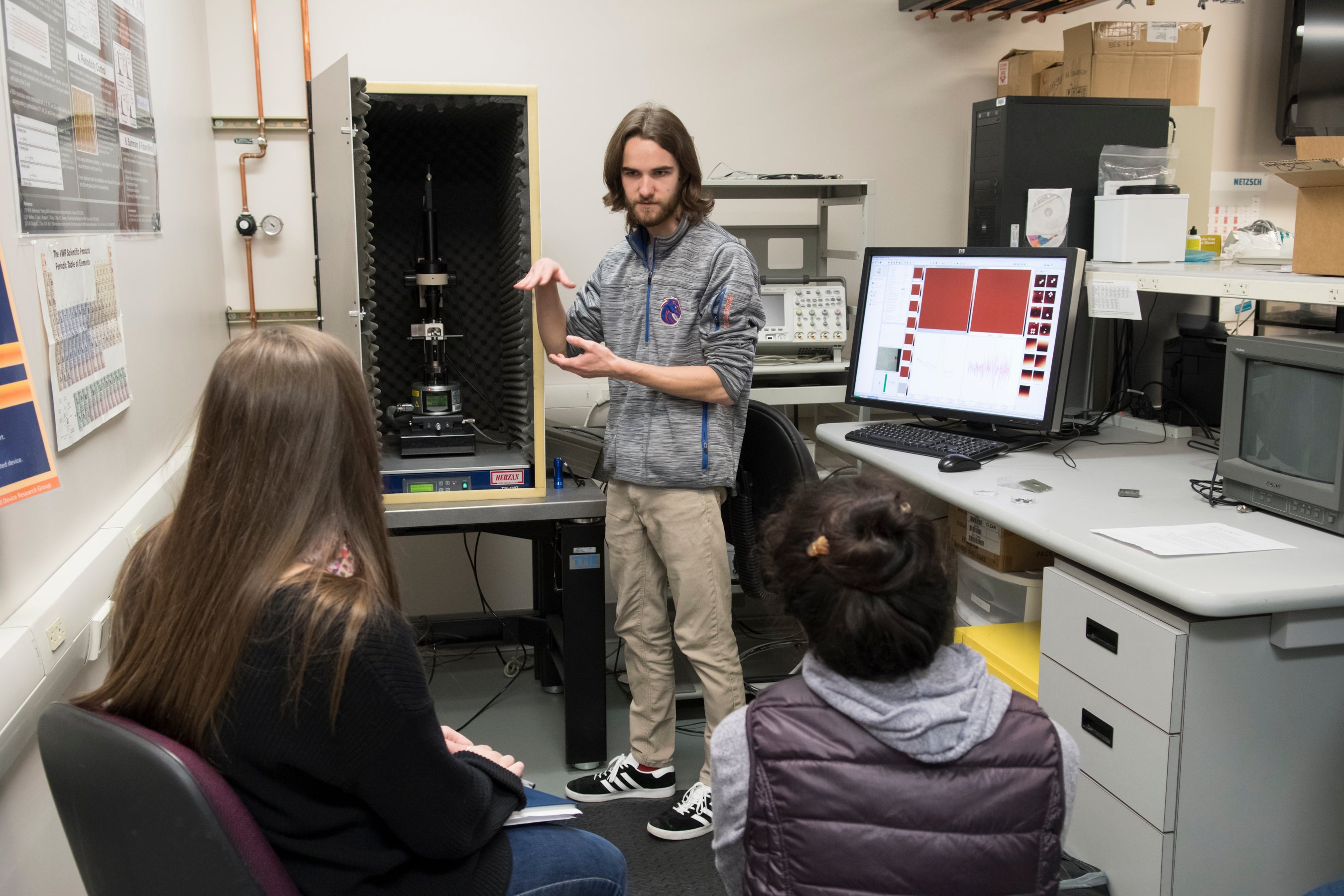
“The focus of the materials science and engineering junior lab curriculum (MSE 381 – Materials Analysis Lab) is to build the knowledge and skills that will make them competitive and successful in whatever they do after graduation,” Ackler explained. “Paul and his team provide an excellent introduction to this amazing technology. Students come away understanding the basic operation of an AFM and the numerous materials and physical properties they can measure.”
The Surface Science Lab houses three Bruker AFMs, as well as other cutting-edge technology that engineering students are trained on to become competitive in Boise’s job market and beyond. Locally, Micron Technology Inc. has two Bruker Dimension Icon AFM systems and Hewlett-Packard has one. Davis said that Boise State graduates – in particular, those with experience using the AFMs in the Boise State Surface Science Lab – have gone on to internships in Micron’s lab and to permanent positions elsewhere within the company, and their exposure to, and experience with AFM has been a huge selling point.
“Many Boise State graduates go on to work for Micron, or other tech companies, where the feature sizes on current semiconductor chips are simply too small to see with a standard optical microscope,” Davis said. “Hence AFM is an essential tool for characterizing semiconductor chips, both in Research and Development – such as occurs at Micron’s global headquarters here in Boise – and production floor environments for quality control purposes. AFM is thus a tool that students are likely to encounter in the high-tech workforce, either as a direct user or, more likely, as an internal ‘customer’ who needs to understand how AFM works and what it can tell you.”
AFMs are useful in both the life and physical sciences, and are key materials characterization tools. Not only do students have the opportunity to see and map things too small to be seen with standard light microscopes, by carefully pushing on a sample and then pulling the probe away, students are able to gauge how hard or sticky the surface is – a process that has important medical implications. For instance, using this method, it’s possible to differentiate between cancerous and non-cancerous cells based on differences in their stiffness.
Alternatively, if an AFM probe is electrically conducting or magnetic, students can learn about the electrical or magnetic properties of the sample and map out variations at a very small scale. This helps visualize differences in composition, predict where corrosion is likely to begin, or map out the magnetic “zeroes” and “ones” (north pole up or down) that make up the information stored on a computer hard drive.
Over spring break, the Surface Science Lab added a new AFM to its suite of tools, a Dimension Icon FastScan with advanced electrochemical capabilities. This newest AFM is housed in a controlled environment (dry, inert atmosphere) glovebox to enable corrosion research, sodium/lithium ion battery research, and numerous other new research directions. This environmental AFM is the first of its kind in the entire Pacific Northwest, and comes to Boise State by way of a National Science Foundation Major Research Instrumentation grant.