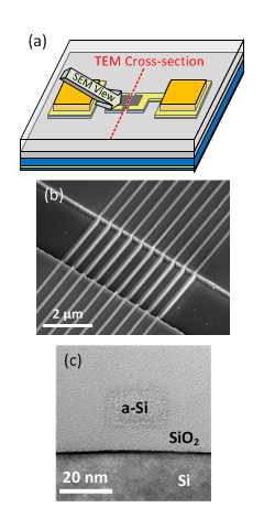
NWFET structures using a-Si:H or nc-Si that could potentially be used for chemical or biological sensors. A scanning electron microscope (SEM) view of a-Si:H nanowires formed in a Schottky barrier TFT channel using electron-beam lithography is shown at right. This image was taken immediately after Cl2-based inductively coupled plasma (ICP) etching of the a-Si:H, but before the PECVD SiO2 capping layer was added. A cross-sectional high-resolution transmission electron microscope (HRTEM) image of a 23 nm wide nanowire in the completed device channel is also shown (below right). Chemical composition of the nanowire was analyzed in-situ using including high-angle annular dark-field scanning transmission electron microscopy (HAADF-STEM) to ensure there was no oxidation or other contamination of the a-Si:H. The perspective of the SEM and location of the TEM cross-section are shown at top right.
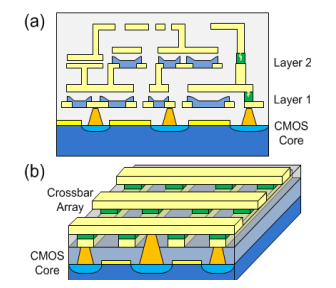
Due to the materials required for interconnects and inter-level dielectrics in the back-end-of-line (BEOL) portion of integrated circuit fabrication, temperatures are limited to <400 °C. Integrating electronic modules into BEOL processes as illustrated in the figure at top right is one way to make more efficient use of Si wafer area. These hardware modules could include learning and adaptation engines powered by neural networks and perform a broad range of tasks. Examples that leverage advanced pattern recognition capabilities include hardware-based detection and correction of faults, errors, or malicious intrusions. Distribution of high-density memory arrays directly over the central processing unit (CPU) could also be used to reduce the latency of information to the processing core. Crossbar arrays are one proposed architecture, requiring two-terminal resistive random access memory (ReRAM) devices at each crosspoint (shown at bottom right). Also known as memristive devices, many different materials exhibit switching behavior.