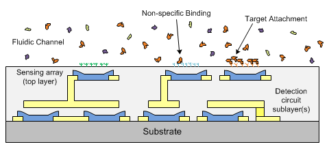
Label-free, affinity-based biological sensing using silicon nanowire field-effect transistors (NWFETs) is promising for point-of-care medical diagnostics. Label-free sensing requires no chemical modification of the target detection species with tags such as fluorescent markers. Affinity-based biosensors take advantage of binding interactions between certain pairs of biomolecules to detect the target analyte, which could be DNA fragments or protein cancer markers. In this scheme, the FET surface is functionalized with receptor molecules and the semiconductor charge (and thus the drain current) of the device is altered when a binding event takes place. Potential advantages of NWFET devices for this application include high sensitivity, near-real-time detection, and good reliability. The overall idea for these systems using low-temperature materials is to fabricate the sensors and underlying detection circuitry directly on large-area, low-cost substrates such as plastic as shown below. Different surface functionalizations placed on each NWFET device in the array will help eliminate errors due to non-specific binding and low signal-to-noise ratio in both gaseous and aqueous environments. Using artificial neural networks as described in the next section to detect the signals is one possibility, as they are good at identifying patterns in noisy signals. The nc-Si TFT circuits discussed previously could also be used for detection techniques based on DC conductance, impedance, or frequency domain analysis.
Nanowire Sensors
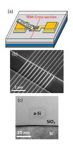
NWFET structures using a-Si:H or nc-Si that could potentially be used for chemical or biological sensors. A scanning electron microscope (SEM) view of a-Si:H nanowires formed in a Schottky barrier TFT channel using electron-beam lithography is shown at right. This image was taken immediately after Cl2-based inductively coupled plasma (ICP) etching of the a-Si:H, but before the PECVD SiO2 capping layer was added. A cross-sectional high-resolution transmission electron microscope (HRTEM) image of a 23 nm wide nanowire in the completed device channel is also shown (below right). Chemical composition of the nanowire was analyzed in-situ using including high-angle annular dark-field scanning transmission electron microscopy (HAADF-STEM) to ensure there was no oxidation or other contamination of the a-Si:H. The perspective of the SEM and location of the TEM cross-section are shown at top right.
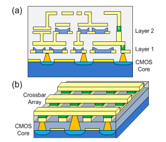
Due to the materials required for interconnects and inter-level dielectrics in the back-end-of-line (BEOL) portion of integrated circuit fabrication, temperatures are limited to <400 °C. Integrating electronic modules into BEOL processes as illustrated in the figure at top right is one way to make more efficient use of Si wafer area. These hardware modules could include learning and adaptation engines powered by neural networks and perform a broad range of tasks. Examples that leverage advanced pattern recognition capabilities include hardware-based detection and correction of faults, errors, or malicious intrusions. Distribution of high-density memory arrays directly over the central processing unit (CPU) could also be used to reduce the latency of information to the processing core. Crossbar arrays are one proposed architecture, requiring two-terminal resistive random access memory (ReRAM) devices at each crosspoint (shown at bottom right). Also known as memristive devices, many different materials exhibit switching behavior.
Resistive Switching Devices (Memristors)
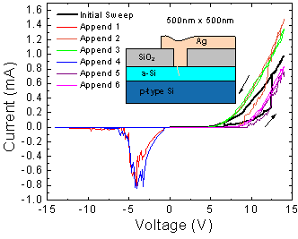
One example is a-Si:H and Ag, desirable because of its compatibility with the nc-Si material previously discussed. The a-Si:H acts as a solid electrolyte in which metal ions will drift and form filaments. Multiple device geometries were fabricated using e-beam lithography, with one set of current-voltage characteristics (and an illustration of the device structure) shown on the left. Since the resistance of the devices change in time, it is difficult to obtain a consistent DC-like measurement. Improved pulse-probe characterization techniques must be used (described below) so that temporal variation of the state variable can be determined precisely. Other materials that operate similarly and are still compatible with nc-Si but rely on a different physical mecanism include HfO2 and TiO2.
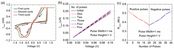
Electrical characteristics of TiN/HfO2/TiN metal-insulator-metal (MIM) structures are shown below. The devices included 5 nm HfO2 dielectric grown on the TiN bottom electrode, which itself is deposited using the physical vapor deposition (PVD) technique. This is followed by a thin Ti film which acts as an oxygen exchange layer generating a certain degree of oxygen deficiency in the metal oxide. The Ti film is capped in-situ by a PVD TiN top electrode. A conductive filament, which is due to a localized highly oxygen deficient region connecting the top and bottom electrodes, can be formed inside the dielectric by either ramping up the applied voltage or using a constant voltage forming method. After forming, application of negative voltage switches the device from a low to a high resistance state (LRS to HRS). Subsequent application of a positive bias makes the device revert back to the LRS. Metal oxidation/reduction processes at the tip of the filaments are primarily responsible for the change in the device resistance. Using slow voltage sweeps of approximately 5 mV/s, hysteresis loops can be obtained as shown below left. Pulse testing can also be employed to quantify the incremental change in conductance. In this scheme, small voltage sweeps like those in above center are used in between the voltage pulses to measure the instantaneous conductance without altering the state. The resistance change resulting from 20 positive followed by 20 negative pulses (1 V, 1 ms duration) is shown below right. This type of switching behavior can be used for digital information storage or as synapses in analog neuromorphic systems. Although such devices are widely investigated for applications in (digital) non-volatile memories, the metrics and design characteristics for neuromorphic applications are somewhat different. It will be important to consider these differences in future device designs.
Synaptic Plasticity
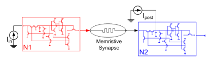
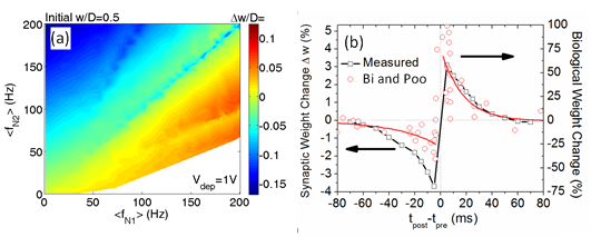
Models of similar memristive devices as well as the ambipolar nc-Si TFTs described previously have been developed using SPICE and used to simulate operation of artificial neural circuits. Advanced learning and signal processing capabilities have been demonstrated in neural network simulations . Both average firing rate Hebbian learning (below left) as well as the more complex but biologically accurate spike timing-dependent plasticity (STDP, below right) mechanisms have been demonstrated. A diagram of the circuit connections used for these experiments is shown below (above the plots). The neuron firing rates and learning algorithms are intentionally designed to closely match biological measurements.
Associative Learning
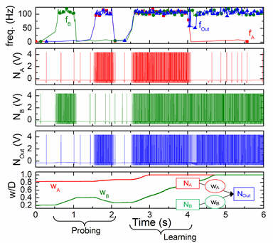
The results of a virtual experiment analogous to Pavlov’s classical conditioning of dogs are shown at right. Two afferent (input) neurons A and B feed into one output. Rapid firing of either A or B represents the sight of food and the sounding of a bell, respectively. Activity of the output neuron represents the salivation response. In dogs, only the sight of the food triggers salivation initially (labeled ‘Probing’ in the figure). After continuous application of the two stimuli (food and bell) for a period of time, only ringing the bell will also invoke the response. This learning stage is also labeled in the figure, followed by the case in which the ‘sight of food’ stimulus is removed but the output remains active. The association will be forgotten by repeatedly presenting the food without ringing the bell. These simulations were performed with an ideal memristive synapse model and average firing rate Hebbian learning rule, but more realistic models produce similar results.
Spatio-Temporal Pattern Recognition
Synaptic learning depends not only on the firing rates of the pre- and post-synaptic neurons, but also on the precise timing difference between action potentials. Typically, potentiation occurs when a pre-synaptic neuron fires right before the post-synaptic neuron, whereas depression occurs in the opposite case. Such STDP is responsible for the ability of animals to quickly respond to threat stimuli, localize sound sources, and learn to recognize and classify temporal patterns and sequences. It has also been known for some time that STDP learning rules enable identification of recurring spike patterns in single layer perceptron networks, even when the duration and recurrence intervals of the patterns are unpredictable. Because the patterns are time-resolved and distributed within a subset of the afferent neurons located in space, this is generally referred to as spatio-temporal pattern recognition.
The figure below shows the firing activity of 25 afferent (input) neurons feeding into one output neuron via memristive synapses as simulated in SPICE. The afferent spike trains have Poisson-distributed inter-spike intervals (left side of the left hand plot). At random times, a fraction (in this case 100%) of the population simultaneously produce unique patterns. These recurring patterns are the same each time they occur for a particular neuron, but are different for each neuron. Spikes that are part of patterns are denoted by open squares in the figure. At first, the output neuron responds randomly to the input spike trains and is not selective to the recurring patterns (right half of left hand plot). Over time (or a certain number of pattern presentations), the synaptic weights are altered such that the output responds only to the occurrence of patterns with very few false detections (right hand plot). The STDP learning rule controls the weight change and there is no supervision or training of the network. Future research will explore how identification of the patterns can be improved, as well as the impact of device physical parameters (e. g. resistance of the memristor, transistor performance/mobility).
