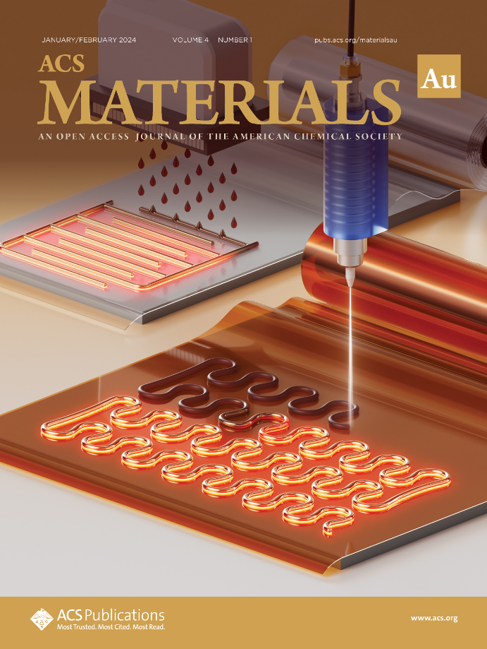
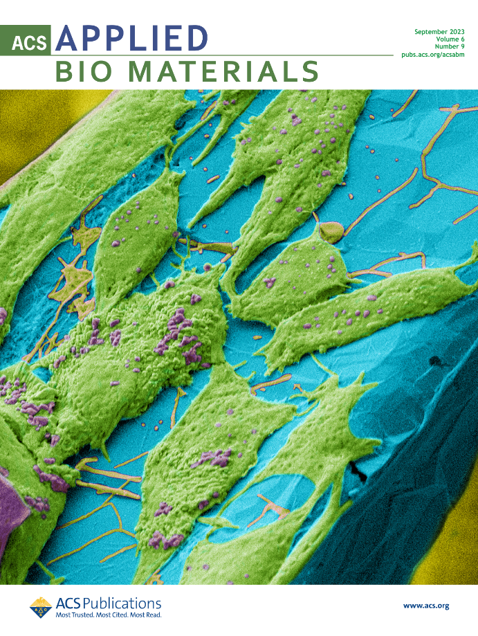
ANML, the Advanced Nanomaterials and Manufacturing Laboratory at Boise State University, takes pride in sharing its publications, each representing a milestone in cutting-edge research and innovation.
Our interdisciplinary team of researchers and collaborators has contributed to leading journals and conferences across various fields, showcasing our commitment to advancing knowledge and addressing real-world challenges.
Recent Publications
-
Thursday Jul 18th, 2024
Assessment of Wafer Scale MoS<sub>2</sub> Atomic Layers Grown by Metal–Organic Chemical Vapor Deposition Using Organo-Metal, Organo-Sulfide, and H<sub>2</sub>S Precursors
Transition Metal Dichalcogenides (TMDs) are a unique class of materials that exhibit attractive electrical and optical properties which have generated significant interest for applications in microelectronics, optoelectronics, energy storage, and sensing. Considering the potential of these materials to impact such applications, it is crucial to develop a reliable and scalable synthesis process that is compatible with modern industrial manufacturing methods. Metal–organic chemical vapor deposition (MOCVD) offers an ideal solution to produce TMDs, due to its compatibility with large-scale production, precise layer control, and high material purity. Optimization of MOCVD protocols is necessary for effective TMD synthesis and integration into mainstream technologies. Additionally, improvements in metrology are necessary to measure the quality of the fabricated samples more accurately. In this work, we study MOCVD of wafer-scale molybdenum disulfide (MoS2) utilizing two common chalcogen precursors, H2S and DTBS. We then develop a metrology platform for wafer scale samples quality assessment. For this, the coalesced films were characterized using Raman spectroscopy, atomic force microscopy, transmission electron microscopy, X-ray photoelectron spectroscopy, and Kelvin probe force microscopy. We then correlate the structural analysis of these grown films with electrical performance by using aerosol jet printing to fabricate van der Pauw test structures and assess sheet resistance. -
Monday Jul 1st, 2024
Infrared AFM as a Technique to Characterize Nanoscale Features
AFM-IR offers a unique approach to analyzing chemical distribution on the nanoscale. Combining the capabilities of atomic force microscopy (AFM) and infrared (IR) spectroscopy, AFM-IR introduces a new level of analysis that was previously unattainable. IR spectroscopy identifies material chemistry by measuring specific IR absorption. AFM measures topographical variation of a wide array of samples, from metals, polymers, ceramics, and biological materials. However, AFM does not allow for material determination, while the spatial resolution of IR spectroscopy is limited to the order of microns in scale. With this tool, anything that is active to IR, meaning it will vibrate when exposed to an IR source, can now be investigated with nanoscale spatial resolution. The ability to analyze material on the nanoscale and decipher its makeup is highly desired in many fields of research, including polymer development, materials degradation processes, alternative energies such as biodiesel, biomedical advancements, and next-generation semiconductor processes. This work is focused on developing an AFM-IR system for usage at Boise State and with collaborators, with successful work presented on an emerging semiconductor process called area-selective deposition via atomic layer deposition. Distinction of nanoscale thin films from a substrate was confirmed with AFM-IR, confirming selective deposition did occur. -
Monday Jul 1st, 2024
Designing a Cell Culture Chamber for the Direct Electrical Stimulation of Mouse Myoblast Cells Grown Ti<sub>3</sub>C<sub>2</sub> MXene Films
Two-dimensional (2D) materials have gained attention for their biocompatibility and limitless applications in regenerative medicine. Of significant interest are the conductive properties of Ti3C2Tx MXene that allow for the direct electrical stimulus (ES) of cells which enhances the tunability of cell differentiation and proliferation. Such advances can be applied to the regeneration of muscle tissue damaged by trauma or wound propagation. The traditional cell culture environment makes it difficult to supply a direct ES to cells without interference from the cell culture media – requiring the design of a cell culture device that facilitates a direct electrode connection to 2D films. This project focuses on the design of a 3D resin-printed chamber that temporarily secures to a glass slide to maintain cell growth on the Ti3C2Tx MXene film which extends outside of the chamber where it contacts the electrodes that supply the direct ES. Our design incorporates a new method of stability, improving the efficiency and reproducibility of experiments by replacing any need for adhesives and allowing for sample characterization without any damaging effects. -
Monday Jul 1st, 2024
Flexible Electrochemical Sensors with Printable Inks to Detect Toxic Heavy Metals
Additive manufacturing of graphene sensors that can measure heavy metals in water offers a sustainable, cost effective and scalable alternative to current sensors available in the market. This study investigates, scalable production of graphene using electrochemical exfoliation, development of graphene inks for extrusion printing and finally develop printed working electrodes on both rigid and flexible substrates for testing. We have demonstrated combining electrochemical and liquid phase exfoliations we were able to develop a scalable production of few layer graphene, achieving resistance in the range of 100 – 400 ohms after annealing at temperature at 300°C. This work shows promise in developing fully printed, flexible and low-cost graphene sensors for heavy metal detection. -
Monday Jul 1st, 2024
Additive Manufacturing of Embedded Sensors for Fluidic Properties Determination in Porous Media
Porous media is used in many industries with applications ranging from chemical catalytic reactors to underground hydrogen storage. Although tremendous research has been done on fluid flow through porous media, there remains a need to develop robust embedded sensors to actively monitor physiochemical properties that affect the myriad applications. Additive manufacturing (AM) is a promising method for the development and fabrication of sensors, due to its ability for rapid prototyping and compatibility with conformal surfaces. However, the industry is limited by the number of commercially available inks, especially for 2D nanomaterials like graphene and MXenes. The novel properties of these materials make them particularly attractive for the development of new sensors, so advancements in AM of 2D inks has the potential to greatly expand the industry. Herein, we examine optimizations in manufacturing of gold, graphene, and MXene nanomaterial inks, AM methods, and production of prototypes for embedded sensors in porous media applications.
Publications Archive
Looking for our older publications? Visit our Publications Archive to view documents spanning from 2008-2022.